
To improve data storage, researchers are perfecting 3D NAND flash memory, which stacks cells to maximize space.
Researchers have discovered a faster, more efficient way to etch deep holes in 3D NAND flash memory using advanced plasma processes. By tweaking the chemistry, they’ve doubled etching speeds and improved precision, setting the stage for denser, higher-capacity memory storage.
Exploring the Future of Data Storage
As electronic devices continue to shrink while handling ever-growing amounts of data, improving the way digital memory is manufactured has become essential. Researchers in a public-private partnership are exploring new methods to create digital memory at the atomic scale, aiming to meet the rising demand for denser data storage.
One major focus is refining the production process for 3D NAND flash memory, a technology that stacks data vertically to maximize storage capacity. A recent study, published in the Journal of Vacuum Science & Technology A, found that using the right combination of plasma and other key materials can double the speed at which the deep, narrow holes essential for this memory are etched. The study was conducted through simulations and experiments by scientists from Lam Research, the University of Colorado Boulder, and the U.S. Department of Energy’s Princeton Plasma Physics Laboratory (PPPL).
NAND flash memory is a type of nonvolatile storage, meaning it retains data even when power is lost. “Most people are familiar with NAND flash memory because it’s the kind that is in the memory cards for digital cameras and thumb drives. It is also used in computers and mobile phones. Making this type of memory denser still — so that more data can be packed into the same footprint — will be increasingly important as our data storage needs grow due to the use of artificial intelligence,” said Igor Kaganovich, a principal research physicist at PPPL.

Stacking Memory Cells to Save Space
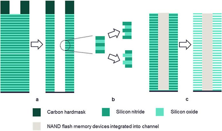
Digital memory saves information in units called cells. Data is saved as the cell’s state, where each cell is either on or off. With traditional NAND flash memory, the cells are arranged in a single layer. In 3D NAND flash memory, many memory cells are stacked on top of each other to fit more data in a smaller footprint. It’s akin to replacing a bungalow with a 10-story apartment to house more people.
A critical step in creating these stacks involves carving holes into alternating layers of silicon oxide and silicon nitride. The holes can be etched by exposing the layered material to chemicals in the form of plasma (partly ionized gases). Atoms in the plasma interact with atoms in the layered material, carving out the holes.
Researchers want to refine how they make these holes so each one is deep, narrow and vertical, with smooth sides. Getting the recipe just right has been tough, so scientists have continued to test new ingredients and temperatures.
Using Plasma to Create Deep, Narrow Channels
“These processes use plasma as a source of high-energy ions,” said Yuri Barsukov, a former PPPL researcher now working at Lam Research. Using the charged particles found in plasma is the easiest way to create the very small but deep, circular holes needed for microelectronics, he said. However, the process, known as reactive ion etching, isn’t fully understood and could be improved. One recent development involves keeping the wafer — the sheet of semiconductor material to be processed — at a low temperature. This emerging approach is called cryo etching.
Traditionally, cryo etching uses separate hydrogen and fluorine gases to make the holes. The researchers compared results from this process to a more advanced cryo-etching process that uses hydrogen fluoride gas to create the plasma.
“Cryo etch with the hydrogen fluoride plasma showed a significant increase in the etching rate compared to previous cryo-etch processes, where you are using separate fluorine and hydrogen sources,” said Thorsten Lill of Lam Research. Headquartered in Fremont, California, Lam Research supplies wafer fabrication equipment and services to chipmakers.
Doubling Etch Rates with New Approaches
When silicon nitride and silicon oxide were tested separately, the etch rate increased for the nitride and the oxide layer using the hydrogen fluoride plasma instead of the separate hydrogen and fluorine gases. While the effect for silicon nitride was more pronounced than for silicon oxide, etching both materials simultaneously yielded the most significant increase. In fact, the etching rate for the alternating silicon oxide and silicon nitride layers more than doubled, increasing from 310 nanometers per minute to 640 nanometers per minute. (A human hair is roughly 90,000 nanometers in width.)
“The quality of the etch seems to have improved as well, and that’s significant,” Lill said.
The researchers also studied the impact of phosphorus trifluoride, an essential ingredient when etching silicon dioxide at any significant degree. While it has been used before, the researchers wanted to better understand and quantify its impact. They found that adding phosphorus trifluoride quadrupled the etch rate for silicon dioxide, though it only marginally increased the silicon nitride etch rate.
Another chemical compound the researchers studied was ammonium fluorosilicate, which forms during the etching process when the silicon nitride reacts with the hydrogen fluoride. The research showed that ammonium fluorosilicate can slow down etching, but water can offset this effect. According to Barsukov’s simulations, water weakened the ammonium fluorosilicate bonds. “The salt can decompose at a lower temperature when water is present, which can accelerate etching,” Barsukov said.
Laying a Foundation for Future Research
Kaganovich said the research is also important because it shows how scientists in industry, academia, and national laboratories can work together to answer important questions in the microelectronics field. It also brings together information gathered from experimentalists and theorists.
“We are building bridges to the greater community,” he said. “This is an essential step in gaining a better understanding of semiconductor manufacturing processes for everyone.”
Lill said he appreciates working with PPPL on semiconductor manufacturing research because PPPL research offers a range of capabilities in plasma simulation for microelectronics.
Reference: “Low-temperature etching of silicon oxide and silicon nitride with hydrogen fluoride” by Thorsten Lill, Mingmei Wang, Dongjun Wu, Youn-Jin Oh, Tae Won Kim, Mark Wilcoxson, Harmeet Singh, Vahid Ghodsi, Steven M. George, Yuri Barsukov and Igor Kaganovich, 18 November 2024, Journal of Vacuum Science & Technology A.
DOI: 10.1116/6.0004019
Funding for this research was provided by PPPL’s Laboratory Directed Research and Development program.